Key takeaways
- Samsung Q3 operating profit hits record ₩107T
- Google Cloud revenue doubles as TPU sales kick in
- Marvell reportedly in talks to buy Lumentum
- US DOJ scrutinizes Nvidia's Hugging Face deal
- TSMC buys AUO LCD fab in Taichung for NT$38.8B
- China's CXMT pushes HBM3E despite 20-30% yields
- 2027 server CPU shipments forecast to jump 46%
Watch the video briefing (in Korean)
More briefing videos on our YouTube channel.
1. Samsung Q3 operating profit hits a record ₩107 trillion on rising memory prices
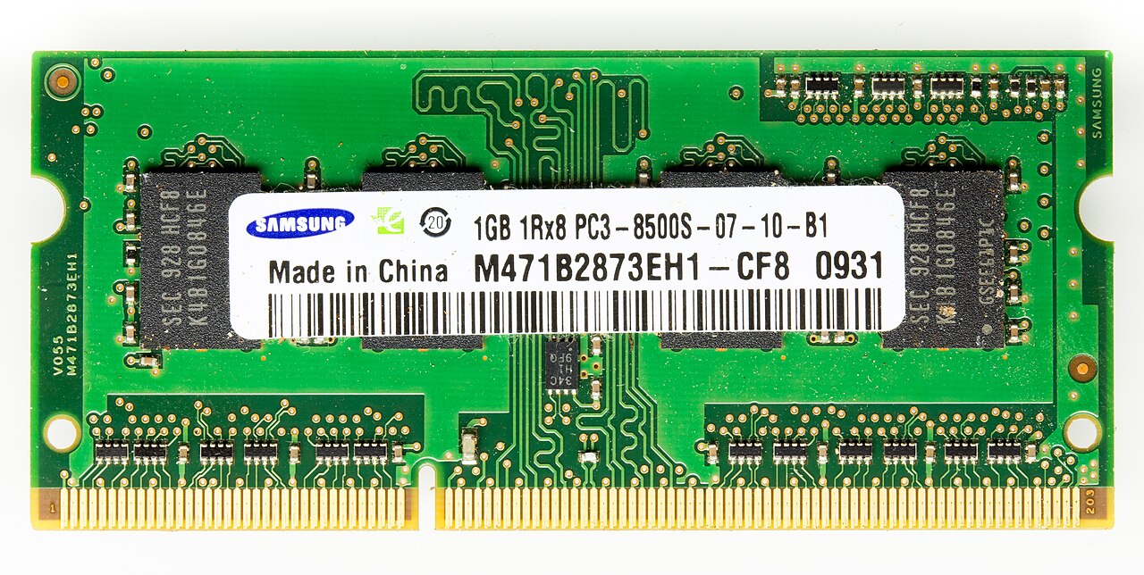
Samsung Electronics reported final third-quarter results on October 29. Consolidated revenue reached ₩195.3 trillion and operating profit ₩107.4 trillion, both all-time highs. The semiconductor (DS) division alone earned ₩106.5 trillion on ₩147.1 trillion in sales, accounting for nearly all of the profit.
On the earnings call, Samsung said its average DRAM selling price rose about 20% from the prior quarter and NAND prices climbed in the high teens. Prices rose across every application, led by servers, and demand keeps outrunning added supply. The company expects memory supply to stay tight in 2028, said next year's HBM output is already sold out, and plans to start mass production of HBM4E in the first half of next year.
Why it matters: Higher prices, more than higher volumes, drove the profit. With the world's largest memory maker expecting shortages through 2028, cost pressure on PCs, phones and other memory-hungry devices may persist.
- ASP (average selling price): The average price of units sold over a period, a key gauge of memory market conditions.
- HBM (high-bandwidth memory): Stacked DRAM that moves large amounts of data at once, mounted next to AI accelerators.
2. Google Cloud revenue up 103% as TPU sales contribute; inventory swells to $13.3B
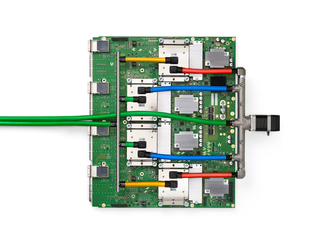
Alphabet reported third-quarter results on October 28. Revenue rose 25% to $127.6 billion, and Google Cloud revenue more than doubled to $30.7 billion. The company said sales of complete systems built on its in-house TPU AI chips were a meaningful contributor to growth.
Inventory reached $13.3 billion at the end of September, up from $2.4 billion at the end of 2025. Executives said TPU inventory is built only after sales contracts are signed and is all tied to committed deals, with a meaningful revenue ramp expected in 2027. They cited work with Anthropic as part of the TPU business but did not break out margins for TPU sales. A day earlier, on October 27, Oracle announced it will offer TPUs in its cloud starting in 2027.
Why it matters: Google is becoming a merchant chip supplier and a direct rival to Nvidia. Because it ties up cash buying hardware in advance, how profitable the business is remains to be proven.
- TPU: Google's custom chip designed for AI workloads.
3. Marvell reportedly in advanced talks to acquire Lumentum
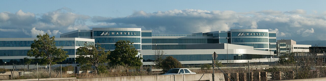
Bloomberg reported on October 28 that chip designer Marvell is in advanced talks to buy optical components maker Lumentum. An all-stock deal is under discussion and could be announced as early as the first week of November. Lumentum is valued at roughly $83 billion.
Neither company has confirmed the talks, and Bloomberg noted they could still fall apart. Marvell makes optical DSP chips for data centers, while Lumentum supplies lasers and optical switches.
Why it matters: Demand for optical links between AI servers is surging. A deal would let Marvell sell everything from DSPs to lasers and compete more directly with Broadcom.
- DSP (digital signal processor): A chip that converts and cleans up high-speed signals carried over fiber.
4. US Justice Department examines Nvidia's $12.9B Hugging Face acquisition

Reuters reported on October 28 that the US Justice Department is examining Nvidia's $12.93 billion purchase of Hugging Face, the largest platform for sharing and distributing AI models. Officials are said to be weighing whether the deal would give Nvidia control over a key distribution point for AI models that it could use against rivals.
According to Reuters, the inquiry is part of a broader review of Nvidia's acquisitions, investments and sales practices. Nvidia has said Hugging Face will keep supporting a range of chip and cloud providers, and it aims to close the deal in the first half of 2027. An investigation does not imply wrongdoing.
Why it matters: As AI competition spreads from chips to software and developer ecosystems, regulators are watching chipmakers' software deals more closely.
5. TSMC buys AUO's Taichung LCD fab for NT$38.8 billion
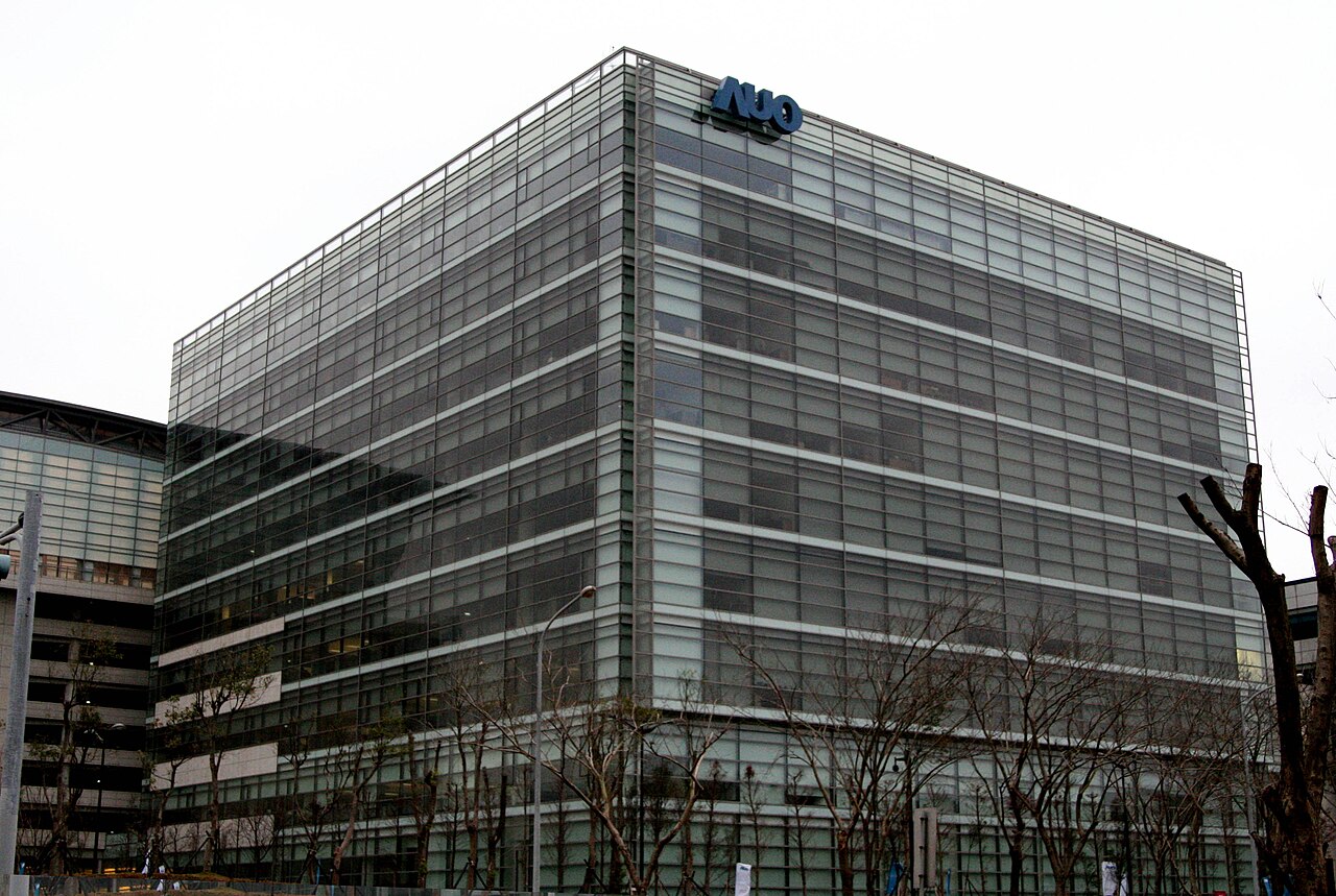
TSMC said in an October 29 filing that it will buy factory buildings, cleanrooms and related facilities in the Central Taiwan Science Park in Taichung from display maker AUO for NT$38.8 billion before tax. The buildings cover about 429,000 square meters. AUO's board approved the sale the same day and expects a disposal gain of about NT$18.5 billion.
TSMC said only that the site will be used for operations and production. Some expect it to host advanced packaging such as CoWoS, but the company has not confirmed that.
Why it matters: Buying an existing display fab gives TSMC buildings and cleanrooms far faster than building from scratch. It bought an LCD plant from Innolux in 2024 for similar reasons.
- CoWoS: TSMC's advanced packaging that places AI chips and HBM side by side on one substrate so they work as a single chip.
6. China's CXMT moves ahead with HBM3E despite 20-30% yields
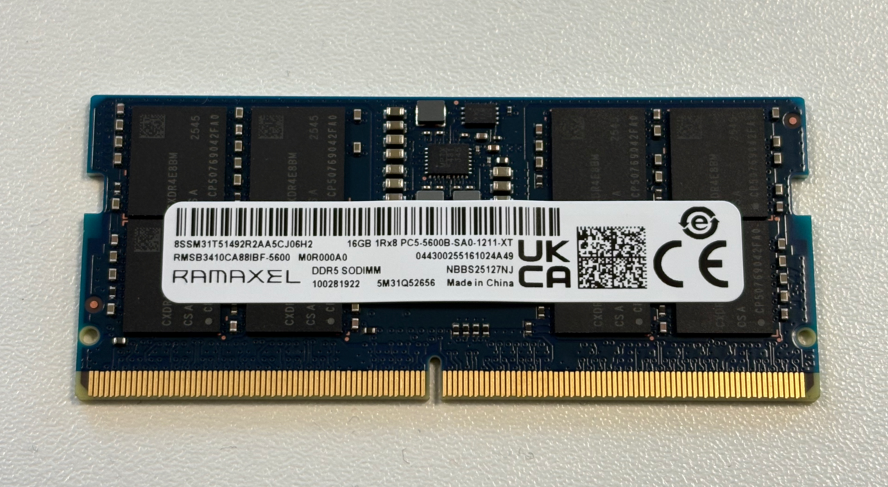
Reuters reported on October 28 that CXMT, China's largest DRAM maker, plans small-scale HBM3E production within two months. The company has reportedly shipped samples to several Chinese AI chip designers.
Initial yields are said to be 20% to 30%, far below the roughly 70% attributed to SK hynix. One source said the part performed closer to SK hynix's previous-generation HBM3 in testing. CXMT has not publicly confirmed the yield figures.
Why it matters: US export controls make it hard for China to buy foreign HBM, so Beijing is prioritizing a domestic supply of AI memory even at high cost.
- Yield: The share of manufactured chips that work properly.
7. Intel CTO says the process gap with TSMC is down to a few points, but scale still lags
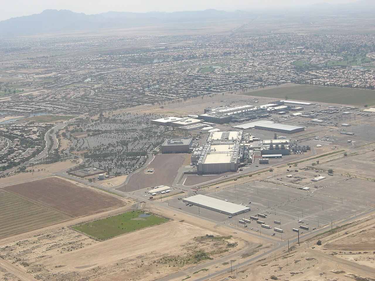
Intel's chief technology officer said the company's process technology now trails TSMC by only a few percentage points, in a special episode of Dwarkesh Patel's podcast recorded during a two-day tour of Intel's fabs and labs. DIGITIMES reported the remarks on October 28.
He acknowledged, however, that matching TSMC's manufacturing scale will take much longer. Yield, capacity and on-time delivery, not just design metrics, decide the foundry race.
Why it matters: Intel wants to build chips for outside customers. To win them away from TSMC, it must prove it can deliver at volume, not just match the technology.
- PPA: Performance, power and area, the standard yardsticks for comparing chip process technologies.
8. Intel to acquire Israeli quantum software firm Classiq
Intel announced on October 26 that it will acquire Classiq, an Israeli quantum computing software company. Terms were not disclosed, but Bloomberg put the price at about $2.3 billion. The deal is expected to close in the first half of 2027.
Classiq's platform automatically turns high-level algorithms into quantum circuits. Intel plans to pair it with its silicon spin-qubit hardware to offer a full-stack quantum platform, while continuing to support Classiq's integrations with other vendors' hardware.
Why it matters: Intel is positioning quantum computing as a long-term growth pillar alongside CPUs and GPUs. Software that makes quantum machines usable matters as much as the hardware.
- Silicon spin qubit: A qubit that stores quantum information in the spin of an electron inside a silicon chip made with conventional processes.
9. 2027 server CPU shipments forecast to rise 45.7%, with AMD set to top Intel in revenue
DIGITIMES Research forecasts global server CPU shipments of 52.6 million units in 2027, up 45.7% year on year, driven by agentic AI, expanding AI servers, cloud giants' in-house CPUs and replacement of general-purpose servers.
Intel is expected to keep the top spot by units with 39%, with AMD closing in at 30.4%. By revenue, AMD is projected to reach $31.2 billion, ahead of Intel's $28.7 billion. Separately, TrendForce said on October 22 that 2027 server CPU shipments would grow by more than 40%.
Why it matters: AI is lifting demand not only for GPUs but for the CPUs that orchestrate them, and the long Intel-dominated server CPU market is being reshaped.
10. ASE lifts 2026 capex again to $11.5B; co-packaged optics enter volume production
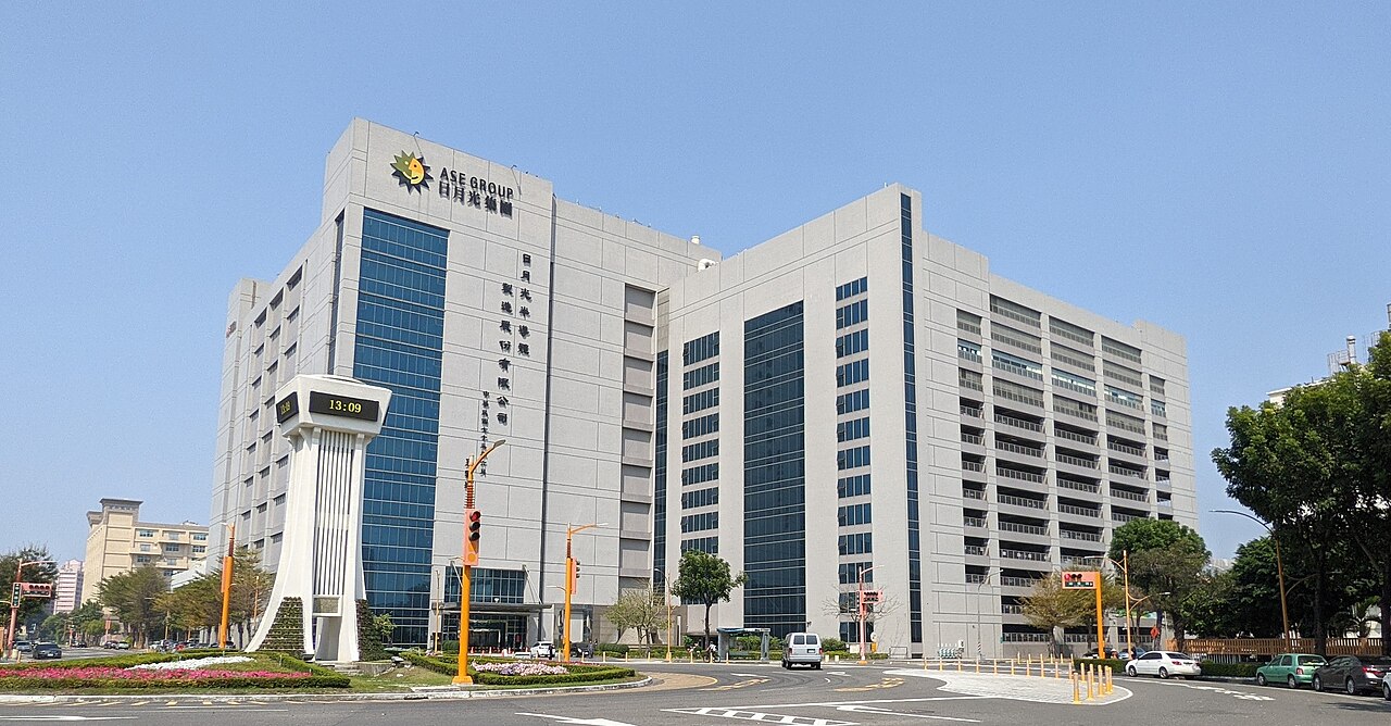
ASE, the world's largest chip packaging and testing company, raised its 2026 capital spending plan from $10.5 billion to $11.5 billion at its October 29 earnings call. The extra $1 billion will be split between buildings and equipment, with about 60% going to its leading-edge advanced packaging and test (LEAP) business. Spending in 2027 will be higher still.
ASE raised its 2026 LEAP revenue target from $3.7 billion to more than $4 billion and expects it to double again in 2027. Co-packaged optics (CPO) entered volume production in the fourth quarter, with more than $500 million in CPO revenue expected in 2027.
Why it matters: AI chips cannot be built without advanced packaging that combines multiple dies. Rising packaging investment shows this step is still a bottleneck.
- CPO (co-packaged optics): Placing optical components inside the same package as the chip to cut power use and signal loss.
11. Samsung Electro-Mechanics Q3 operating profit up 165%; MLCC long-term deals with about 50 customers

Samsung Electro-Mechanics posted record quarterly revenue of ₩3.7633 trillion and operating profit of ₩691 billion, up 165% from a year earlier. The component division, which makes MLCCs, grew revenue 36% to ₩1.883 trillion, and the package solution division, which makes FC-BGA substrates, rose 58% to ₩939 billion.
On the earnings call, the company said it has signed or is negotiating long-term MLCC supply agreements with about 50 customers. With capacity short of demand and raw material costs rising, it is negotiating prices with customers.
Why it matters: AI servers use far more MLCCs and larger, more complex substrates than ordinary servers. As customers rush to lock in supply, component makers are gaining pricing power.
- MLCC (multilayer ceramic capacitor): A tiny component that stores and releases charge to keep circuit voltage stable.
- FC-BGA: A substrate that connects high-performance chips to the motherboard.
12. TI and NXP see industrial chip recovery, with industrial sales up 40% and 39%

Texas Instruments' third-quarter revenue rose 28% to $6.06 billion, with growth across industrial, automotive and data center markets; on the earnings call it said industrial revenue grew more than 40%. It guided fourth-quarter revenue to $5.80 billion to $6.30 billion.
NXP reported third-quarter revenue of $3.79 billion on October 27, up 19%. Industrial and IoT revenue rose 39% to $802 million, which the company attributed to AI-enabled processors, data centers and factory automation.
Why it matters: Industrial chips suffered a long inventory correction in 2023-2024. Data center power equipment and factory automation are now driving a clear rebound.
- Analog chip: A chip that handles continuous signals such as voltage, current or temperature, used in power management and sensing.
13. Silicon Motion Q3 revenue reaches $560M, up 131% year on year

SSD controller maker Silicon Motion reported third-quarter revenue of $560.2 million, up 131% from a year earlier and 24% from the prior quarter. Gross margin was 53.6% and operating margin 29.0%.
The company said its 4nm PCIe Gen 6 MonTitan controllers for enterprise and AI SSDs are beginning to scale. It guided fourth-quarter revenue to $588 million to $616 million.
Why it matters: AI data centers consume large volumes of high-performance SSDs, and that demand is spreading from memory chips to the controllers that manage them.
- SSD controller: The chip inside an SSD that manages reading and writing data to NAND flash.
14. Fire hits Taiwan power-chip wafer maker Episil; less than 10% of capacity affected
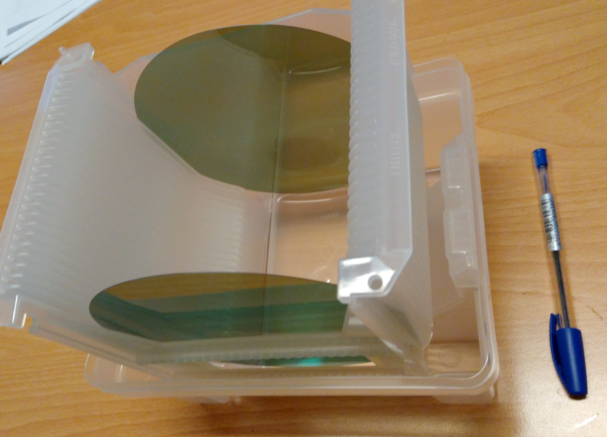
A fire broke out on the morning of October 28 in a cleanroom at Episil-Precision's Innovation plant in Hsinchu Science Park. All 92 people inside were evacuated without injury, and the blaze was put out in about three hours. About 3,700 square meters burned, with damage initially estimated at NT$130 million.
On October 29 the company said the affected area accounts for less than 10% of total capacity and output, and that it has activated backup production at other plants. It said it is fully insured. Fire officials are investigating the cause.
Why it matters: Episil makes epitaxial wafers used as the base for power semiconductors. The company says the impact is limited, but with few suppliers of this material, customers are watching the recovery.
- Epitaxial wafer: A wafer with an extra thin crystal layer grown on top, used to improve the performance of power chips and other devices.
15. Taiwan's LandMark to boost silicon photonics laser capacity 2.5-fold in 2027
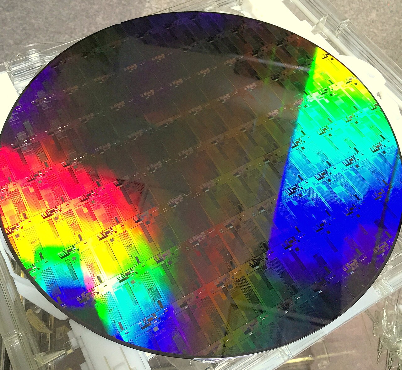
Taiwanese optical materials maker LandMark Optoelectronics plans to lift its 2027 capacity for CW lasers used in silicon photonics to 2.5 times the 2026 level, and hopes to keep a similar pace of expansion in 2028. It described current capacity as very tight.
Its board approved equipment spending of up to NT$2.27 billion, and the company signed a four-year CW laser supply contract covering 2027-2030 with a US customer.
Why it matters: Silicon photonics and CPO chips rely on external lasers for their light source. As optical links in AI data centers multiply, these lasers could become a new bottleneck.
- Silicon photonics: Building optical pathways on silicon chips so data moves as light rather than electricity.
- CW laser: A laser that emits light continuously, used as the light source for silicon photonics chips.
16. LB Semicon expands power-chip packaging capacity on a 10-year Qualcomm deal

Korean chip packaging company LB Semicon will invest about ₩30 billion to expand capacity under a 10-year supply agreement with Qualcomm. By 2028 it plans to raise 200mm-equivalent capacity at its Pyeongtaek headquarters from 26,000 to 36,000 wafers a month and 300mm capacity from 3,000 to 5,000 wafers a month.
The agreement took effect in February 2026 and renews automatically every two years. It does not fix volumes in advance; LB Semicon supplies Qualcomm's orders within its available capacity. The company began volume shipments of Qualcomm power management ICs (PMICs) in August.
Why it matters: It shows a Korean back-end firm long dependent on display driver chips moving into a global chipmaker's supply chain to diversify.
- PMIC (power management IC): A chip that delivers the right voltage and current to each part of a device.
17. Taiwan's Kinsus explores aluminum nitride ceramic as AI chip substrates grow larger
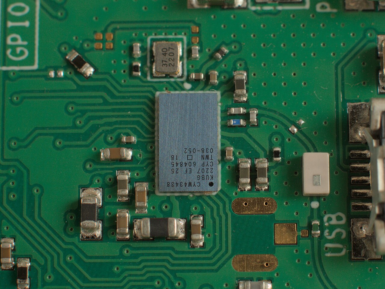
Lin Ding-hao, R&D vice president at Taiwanese substrate maker Kinsus, discussed materials for advanced packaging substrates at the TPCA Show in October. As AI chip packages grow, keeping substrates flat, dimensionally stable and resistant to warping becomes a central challenge.
He noted that glass cores, a leading next-generation candidate, have attractive material properties but are brittle and hard to make reliable. Kinsus is therefore researching aluminum nitride (AlN) ceramic, which conducts heat well, as a substrate material.
Why it matters: AI chips put more dies and memory on a single substrate, so substrates keep getting bigger. Warping under heat causes defects, sparking a race among glass, ceramic and other new materials.
- Warpage: Bending of a substrate caused by chips and substrate expanding at different rates (CTE) when heated.
- Glass core substrate: A next-generation substrate whose core layer is glass instead of organic material, making it flatter and less prone to warping.
18. Nvidia reportedly weighing microchannel cooling for Rubin Ultra
Reports continue to suggest that Nvidia's next-generation Rubin Ultra AI chip may use microchannel cold plates (MCCP) that run coolant directly above the die. With power per chip possibly reaching 2,300W, conventional cold plates may struggle, and Taiwanese cooling firm AVC has been named as a partner.
According to SemiAnalysis, the Rubin GPU's cold plate already uses a microchannel design with channel pitch narrowed from 150 microns to 100 microns (0.1mm). Nvidia has not officially confirmed the final cooling design for Rubin Ultra.
Why it matters: As AI chip power keeps climbing, cooling is becoming part of package design rather than just a facility issue.
- Microchannel cooling: Running coolant through hair-thin channels to remove large amounts of heat from a small area.
Sources
- 삼성전자, 반도체서만 106조5000억 이익…"내년 HBM 이미 완판" (디일렉)
- [컨콜] 삼성전자 "메모리 공급 부족 2028년까지 지속" (EBN)
- [컨콜] 삼성전자 "메모리 공급 부족 2028년까지, HBM4E 내년 상반기 양산" (뉴스웍스)
- 삼성전자, 분기 영업익 107조 '새 역사'⋯HBM4 타고 반도체 초호황 질주 (이투데이)
- Alphabet Announces Third Quarter 2026 Results (Exhibit 99.1) (Alphabet / SEC)
- Alphabet (GOOGL) Q3 2026 Earnings Call Transcript (The Motley Fool)
- Stock Market Today, Oct. 29: Marvell Falls on Lumentum Acquisition Talks (The Motley Fool)
- Marvell Is Reportedly in Advanced Talks to Buy Lumentum for Its AI Optics (Startup Fortune)
- Marvell Stock: Why Lumentum Deal Makes It Look Like Broadcom (Benzinga)
- Nvidia faces DOJ antitrust scrutiny over $12.9B Hugging Face deal, Reuters says (Yahoo Finance (Reuters))
- Nvidia under probe by US justice officials over Hugging Face acquisition (DIGITIMES)
- DOJ looks into Nvidia's $12.9B Hugging Face deal, Reuters reports (The Next Web)
- 台積電斥資388億元 買下友達中科廠 (自由財經)
- 台積電砸388億元買友達中科廠 取得近13萬坪廠房 (經濟日報)
- 友達中科兩廠388億賣台積 資產活化告一段落 (經濟日報)
- CXMT Reportedly Ships HBM3E Samples, Eyes Production Within 2 Months Despite 20–30% Yields (TrendForce)
- China's CXMT will make AI memory despite yields as low as 20%, Reuters says (The Next Web)
- Intel CTO: process gap with TSMC down to a few points, but scale still lags (DIGITIMES)
- Intel to acquire quantum software company Classiq (Evertiq)
- Intel to buy quantum software firm Classiq for about $2.3bn (The Next Web)
- Intel acquires quantum software firm Classiq for $2.2bn (DatacenterDynamics)
- Server CPU shipments set to surge 46% in 2027, with AMD eyeing revenue crown (DIGITIMES)
- TrendForce Forecasts Server CPU Shipments to Rise More than 40% in 2027 (EE Times Asia)
- 〈日月光法說〉Q4 營收估季增 6-8%、再度追加資本支出 LEAP目標上修明年可望翻倍 (鉅亨網)
- CPO第四季啟動量產、明年營收估逾5億美元!日月光投控2027年LEAP業務看倍增 (風傳媒)
- 日月光投控第四度上修今年資本支出 明年先進封測營收目標倍增 (自由財經)
- 삼성전기, 3분기 역대 최대 실적…반도체 기판·MLCC 수요 폭발 (한국경제)
- 삼성전기 2026년 3분기 실적발표 컨퍼런스콜 전문 (디일렉)
- Texas Instruments Q3 2026 Earnings Release (Exhibit 99) (Texas Instruments / SEC)
- Texas Instruments (TXN) Q3 2026 Earnings Call Transcript (Webull)
- NXP Semiconductors Reports Third Quarter 2026 Results (GlobeNewswire)
- Silicon Motion Announces Results for the Period Ended September 30, 2026 (Exhibit 99.1) (Silicon Motion / SEC)
- 嘉晶:火警影響區域占總產能低於10% 啟動備援機制 (中央社)
- 嘉晶竹科創新廠無塵室火警92人疏散 公司:營運無重大影響 (經濟日報)
- 竹科「嘉晶電子」創新廠火警 財損約1.3億 (自由時報)
- AI帶旺光通訊需求 聯亞獲美客戶長約、擬投22.7億擴充產能 (中央社)
- 聯亞8月營收年增180% 法人估2027產能為今年2.5倍 (優分析)
- LB세미콘, 퀄컴 10년 계약 등에 업고 캐파 월 1만장 증설 (디일렉)
- LB Semicon to expand PMIC capacity under 10-year Qualcomm deal (DIGITIMES)
- Research Insight:AI先進封裝不只玻璃載板? 景碩探索AlN陶瓷材料新路徑 (DIGITIMES)
- TPCA Show 20日登場 PCB結合AI、先進封裝題材 欣興、景碩等海內外大咖齊搶商機 (工商時報)
- Rubin Ultra GPU to Use Advanced Microchannel Cooling for its 2300W TDP (Guru3D)
- Vera Rubin – Extreme Co-Design: An Evolution (SemiAnalysis)
- Vera Rubin液冷也難救?AI晶片熱阻瓶頸難解 散熱三雄高層親揭突圍密技 (工商時報)
Compiled by Bits & Bites from public reporting. Not investment advice.
Leave a Reply