Key takeaways
- SK hynix Q3 revenue hits ₩104.6T with an 80% operating margin
- Customer HBM requests exceed SK hynix's supply by more than 2x
- Google TPUs coming to Oracle Cloud starting in 2027
- AMD to buy $1B of Meta stock in its share offering
- Solidigm drops IPO, keeps pursuing a US NAND fab
- UMC fab utilization climbs to 92% on record revenue
- 3M takes a 4.7% stake in Taiwan optics maker GSEO
Watch the video briefing (in Korean)
More briefing videos on our YouTube channel.
1. SK hynix posts ₩104.6 trillion quarter as HBM orders run at twice its supply
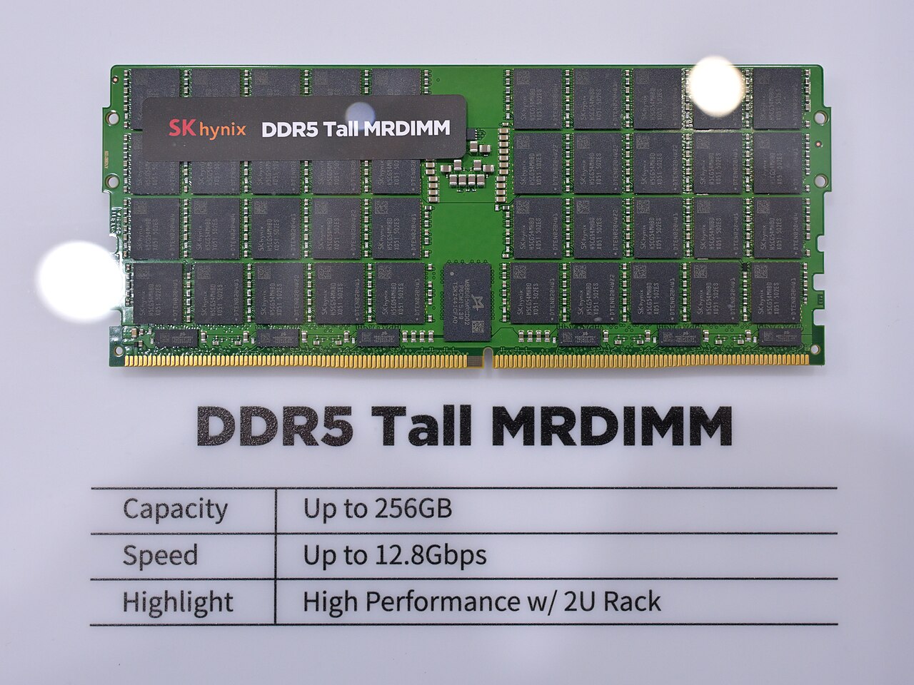
SK hynix reported third-quarter results on October 28. Revenue reached ₩104.6 trillion, crossing ₩100 trillion for the first time, and operating profit came to ₩83.3 trillion, an 80% margin.
On the earnings call, the company said the HBM volume customers are asking for is more than double what it can supply. HBM4 yields came in ahead of plan, so the company raised its targets, and it expects HBM4 to overtake the older HBM3E in both shipments and revenue in the fourth quarter. Asked about customers moving to stacks with fewer layers, it said this does not ease supply, because matching the same capacity requires more stacks.
SK hynix has signed long-term agreements with 14 major customers, including large cloud providers, which lock up more than half of its 2027-2028 capacity.
Why it matters: High-performance memory for AI servers is effectively sold out years ahead. Because memory makers are prioritizing HBM, the squeeze is spilling over into supply of conventional memory as well.
- HBM (high bandwidth memory): DRAM chips stacked in layers to move large amounts of data at once, placed right next to an AI accelerator.
- LTA (long-term agreement): A contract that fixes supply volumes and a price range for several years in advance.
2. Oracle Cloud brings Nvidia, Google TPUs, Cerebras and SambaNova under one roof
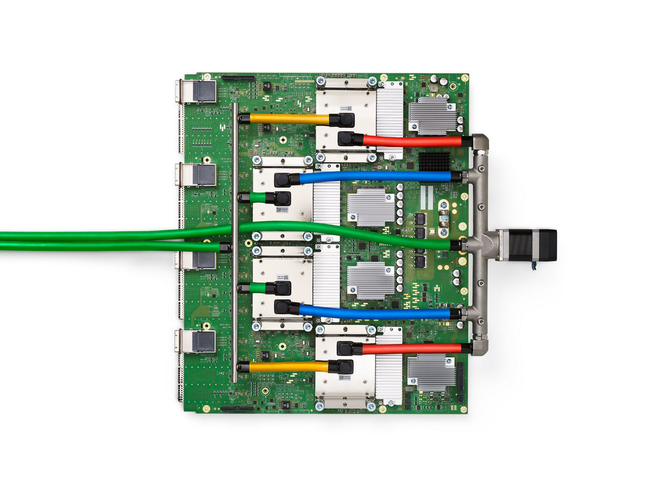
At its AI World 2026 event in Las Vegas on October 27, Oracle said Oracle Cloud Infrastructure (OCI) will offer AI chips from several vendors. Nvidia's Vera Rubin NVL72 racks are now generally available, with plans to scale to multiple gigawatts.
The headline addition is Google's TPU. The TPU 8t for training and TPU 8i for inference will arrive on OCI in 2027 and ramp over several years. The companies say this is the first time a hyperscale cloud outside Google will offer TPUs, with Oracle supplying the power, cooling and networking. Cerebras' wafer-scale inference service (2027) and SambaNova's fifth-generation SN50 chips are also coming to OCI.
The Information reported that OpenAI also plans to buy TPUs, though the companies have not confirmed this.
Why it matters: Until now, Google's TPUs were available only on Google Cloud. Offering them elsewhere widens the menu of alternatives to Nvidia in the AI chip market.
- TPU: Google's in-house chip designed specifically for AI computation.
- Inference: The stage where a trained AI model answers questions or generates output.
3. AMD to buy $1 billion of Meta stock as Helios racks enter testing at Meta

AMD said on October 27 that it will invest $1 billion in Meta's equity offering. Meta plans to raise $95 billion in total for AI infrastructure, and Nvidia has separately committed $3 billion.
AMD said the first Helios rack-scale AI systems are installed at Meta and in testing ahead of broader deployment. In February, the two companies signed a deal for Meta to deploy up to 6 gigawatts of AMD AI hardware.
Why it matters: Chip suppliers and big tech customers are increasingly tied together through cross-holdings, with chipmakers buying customer shares and customers receiving chipmaker equity.
- Rack-scale system: GPUs, CPUs and networking packed into a single server rack that works like one large computer.
4. Solidigm shelves IPO but keeps a $45 billion US NAND fab in play
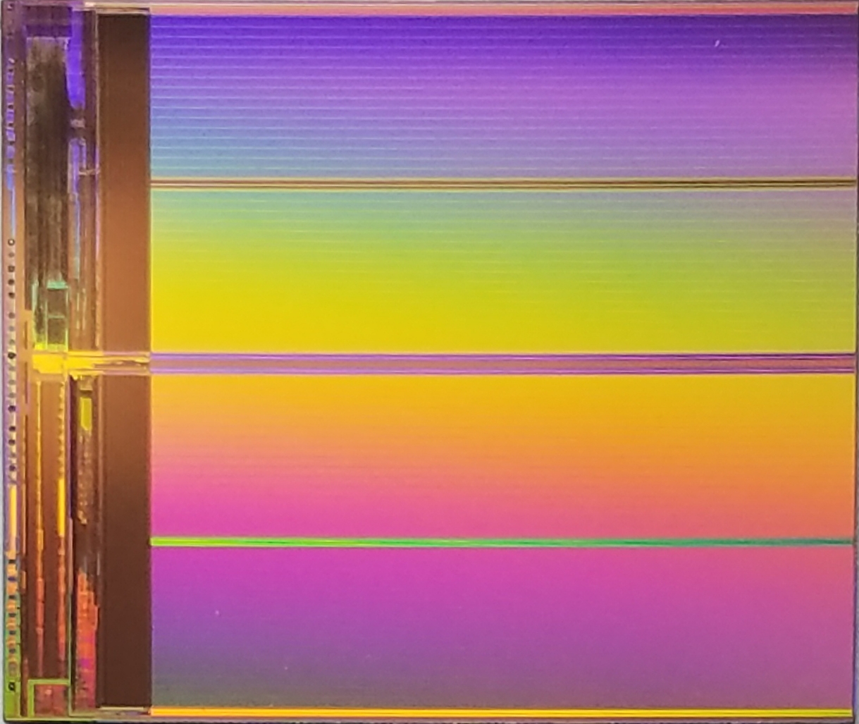
SK hynix said on October 23 that it had stopped reviewing an IPO for its US subsidiary Solidigm, and confirmed the decision again on its October 28 earnings call.
The plan for a new US NAND flash fab continues. Reports say Solidigm is in talks with the US government over a fab investment of about $45 billion. Reuters reported that Solidigm has applied for a US export license to add equipment at its Dalian, China plant (Mod B) and has tied the US fab plan to that license. Korean media say alternatives such as internal cash, corporate bonds, bank loans and outside investors are being discussed for funding.
Why it matters: Washington allows existing China fabs to keep running but does not expect to approve tools for expansion or upgrades. The link between the Dalian license and the US fab is the key variable.
- NAND flash: Storage memory that keeps data without power, used in SSDs and phone storage.
5. SK hynix stretches today's DRAM design with EUV as China's CXMT pushes 4F²
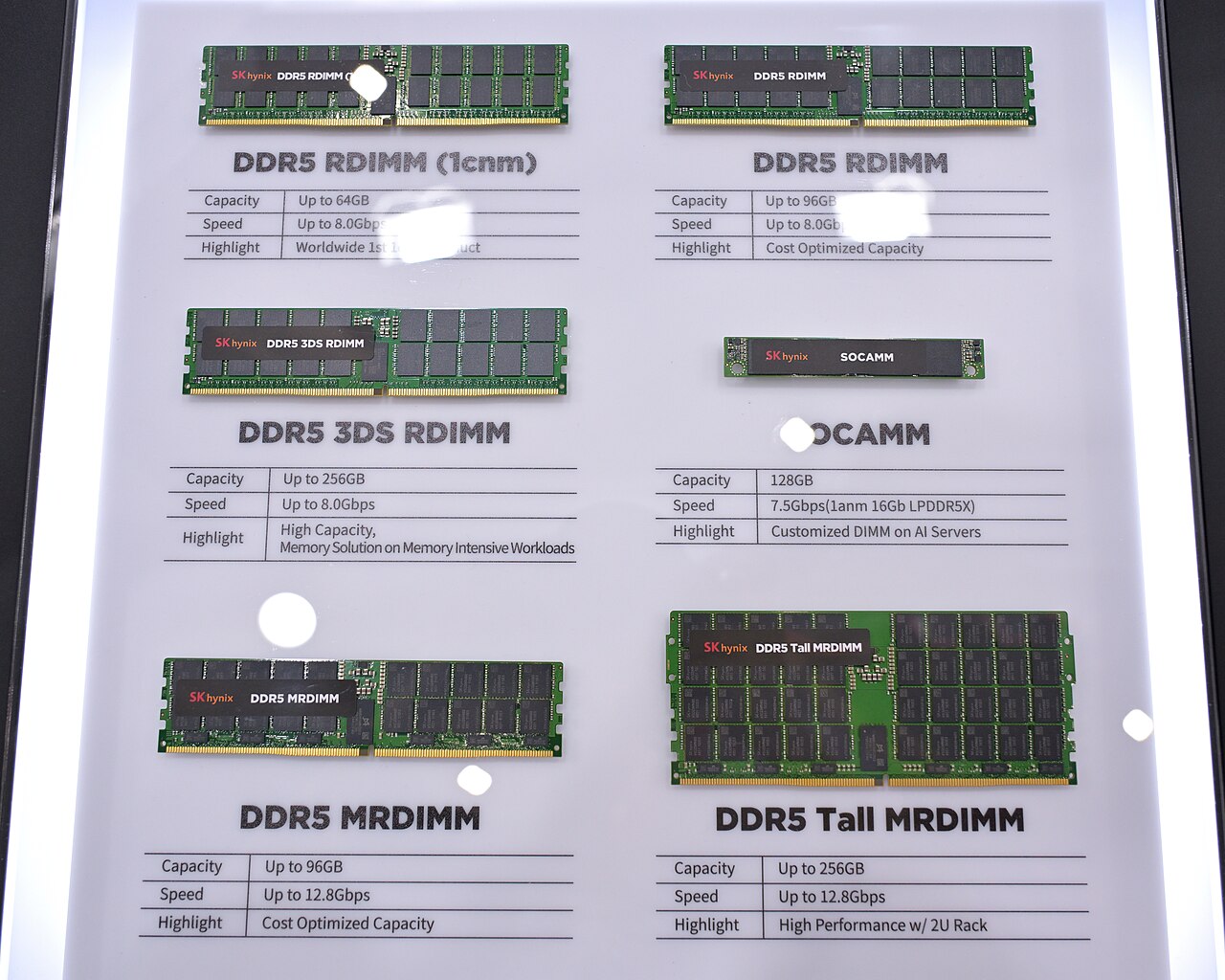
On its October 28 earnings call, SK hynix said it has secured room to extend its current 6F² DRAM cell design through EUV lithography and process innovation. Next-generation 4F² and 3D DRAM will be commercialized only once they meet yield, reliability and cost requirements and pass customer evaluation, not just performance goals.
China's CXMT says it has built vertical surround gate (VSG) transistors and is preparing 4F² server DDR5 modules based on them. Shares of Samsung Electronics and SK hynix fell sharply after that announcement earlier in October.
Why it matters: Export controls keep CXMT from buying EUV tools, so it is changing the cell structure to raise density instead. Memory competition is splitting into an equipment path and an architecture path.
- 6F² / 4F²: The area one DRAM cell occupies; a smaller number means more cells fit in the same space.
- EUV lithography: Chipmaking technology that uses extremely short-wavelength light to print very fine circuits on wafers.
6. SK hynix lays out memory tiers beyond HBM, from HBF to CXL

SK hynix is pitching technologies that reshape memory across the whole AI server, not just HBM. At the OCP Global Summit in San Jose on October 12-15, it showed MARS, a rack-level design that pools memory so servers and GPUs can share it, a 256GB memory module based on CXL 3.2, and CMM-Ax, which performs computation inside the memory.
Around its earnings release, the company also described tiered-memory tools for AI inference. SALT-KV is software that places an AI model's KV cache across HBM, DRAM and SSD based on reuse value and cost, while CMM-Hybrid prefetches data from SSD into DRAM to cut latency. HBF (high bandwidth flash), which stacks NAND in an HBM-like way to sit between HBM and SSDs, is a medium- to long-term development goal.
Why it matters: As AI models grow longer and more complex, HBM alone runs out of capacity. A new tier between costly HBM and cheap SSDs aims to balance speed and cost.
- CXL: An interconnect standard that links CPUs, GPUs and memory quickly so multiple devices can share memory.
- KV cache: Intermediate data a language model stores so it does not have to recompute what it has already processed.
7. UMC runs at 92% utilization as AI demand reaches mature-node foundries
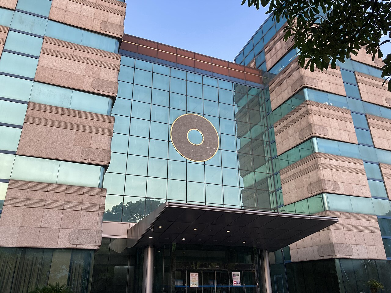
Taiwanese foundry UMC said on October 28 that third-quarter revenue hit a record NT$74.24 billion, up 8.0% from the prior quarter and 25.6% from a year earlier. Fab utilization rose from 85% to 92%, and gross margin was 34.0%.
Several 12-inch fabs were running full and 8-inch fabs recovered. The board approved about $3.2 billion in additional capital spending to speed up expansion in Singapore and Tainan.
Why it matters: AI server demand is keeping busy not only leading-edge lines but also older processes that make chips such as power management ICs.
- Mature node: An older, well-proven manufacturing process, typically 28nm and above.
8. Taiwan chip-test supplier CHPT doubles quarterly profit on AI testing
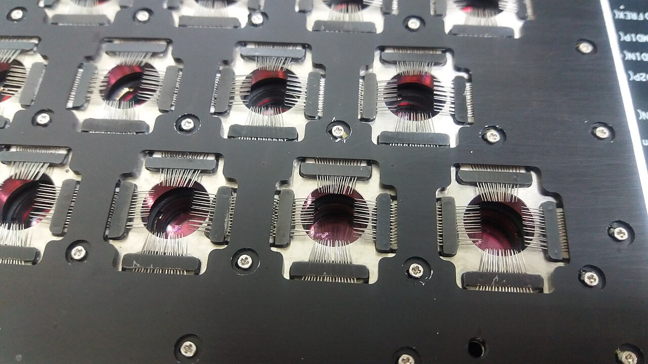
Taiwan's Chunghwa Precision Test (CHPT) reported third-quarter revenue of NT$1.905 billion, up 53.4% year on year, and net profit of NT$551 million, double a year earlier. Both were quarterly records, the third straight quarter of new highs.
Testing demand for AI and high-performance computing drove the growth, and probe card revenue was about NT$400 million.
Why it matters: AI chips are expensive and complex, so testing before shipment is more demanding. As chip demand rises, test-component makers are getting busier too.
- Probe card: A part that touches chips on a wafer with tiny needles to check for defects using electrical signals.
9. Substrate maker Unimicron adds NT$50.9 billion in equipment orders
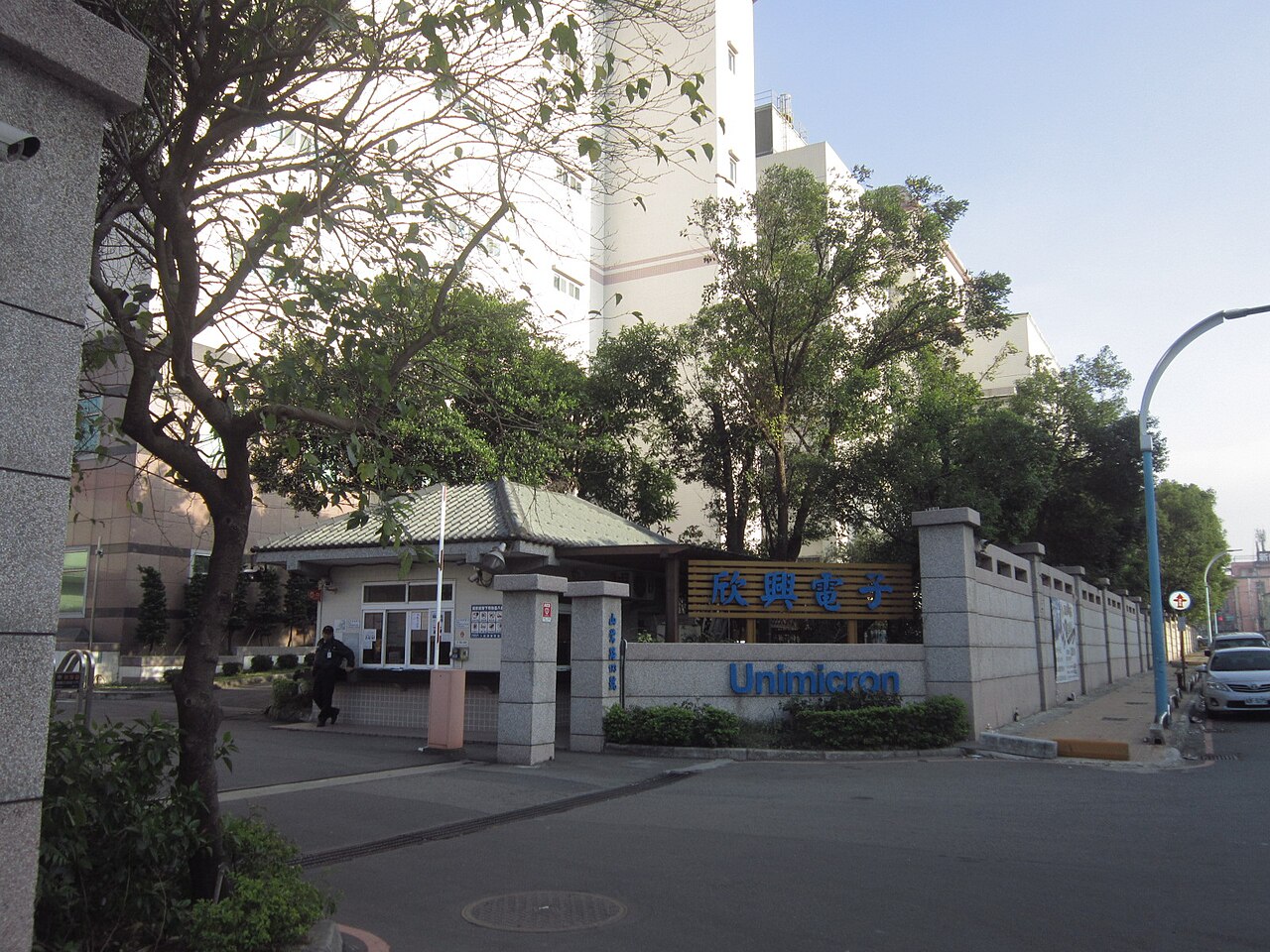
Unimicron, a Taiwanese maker of ABF substrates for AI chips, decided at its October 27 board meeting to add about NT$50.9 billion in advance orders for long-lead equipment. It was the fourth increase this year and the largest.
The board also approved a letter of intent to sell all of its Japanese subsidiary, Unimicron Japan, to Japanese PCB maker Meiko. Third-quarter revenue reached a record NT$52.65 billion.
Why it matters: As AI chips get larger, the substrates beneath them need more area and more layers. Suppliers are racing to add capacity so substrates do not become a bottleneck for AI servers.
- ABF substrate: A package substrate connecting high-performance chips to the motherboard, named after Ajinomoto's insulating film.
10. Simmtech to invest ₩274.2 billion in Cheongju for AI memory module boards
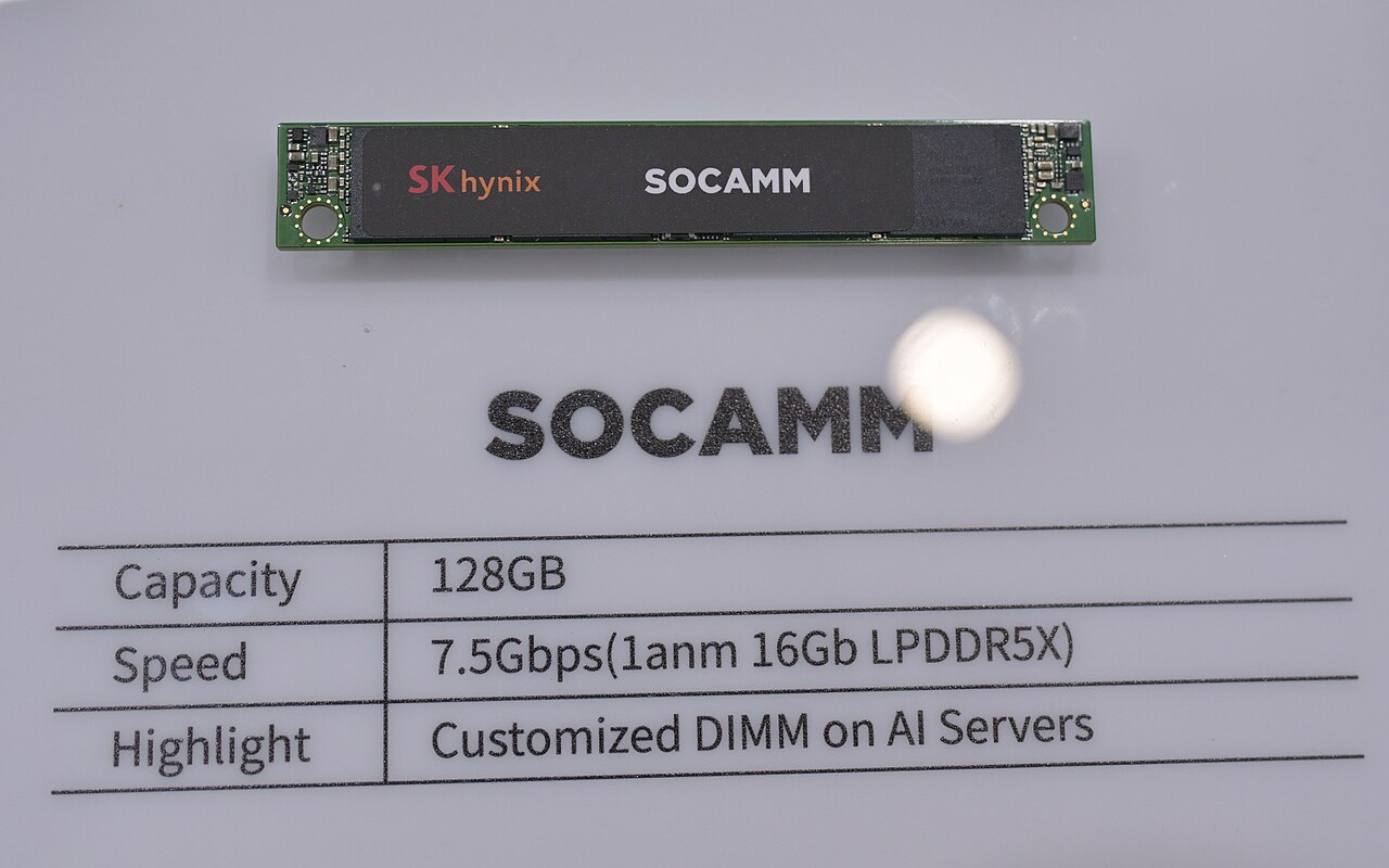
Korea's Simmtech will spend ₩274.2 billion in Cheongju through the end of 2027 to add capacity. Of that, ₩145.9 billion goes to a new plant for SOCAMM module boards used in AI servers, ₩105.1 billion to mSAP package substrates and ₩23.2 billion to substrates for system chips.
Simmtech also signed an investment agreement with North Chungcheong Province and Cheongju city worth ₩400 billion in total, with the ₩274.2 billion as the first phase.
Why it matters: SOCAMM is a new memory module format that Nvidia and others plan to use in AI servers. Demand is rising not only for memory chips but also for the boards they sit on.
- SOCAMM: A small, replaceable server memory module built from low-power DRAM (LPDDR).
- mSAP: A substrate manufacturing method that can produce very fine circuit lines.
11. 3M invests NT$4.8 billion in Taiwan's GSEO for data center optics

3M will acquire about a 4.7% stake in Taiwanese optics maker GSEO (Genius Electronic Optical) and work with it to develop and manufacture expanded beam optical (EBO) products for data centers. According to GSEO's filing, 3M will invest about NT$4.81 billion (around $150 million) through a private placement, with closing expected in the fourth quarter.
GSEO is expected to handle volume production of 3M's EBO ferrules, co-packaged optics and related optical interconnect parts.
Why it matters: Data traffic between AI servers is surging, pushing data centers to replace copper links with optical connections that carry signals as light.
- CPO (co-packaged optics): Packaging the parts that convert electrical signals to light right next to the chip to cut power and latency.
- Ferrule: A small part that holds an optical fiber end in a precise position so fibers line up.
12. TI sees AI data center liquid cooling moving to tray-level control
Patrick Zeng, general manager of data center thermal management at Texas Instruments, told DIGITIMES that liquid cooling in AI data centers is moving toward more granular control.
Today a coolant distribution unit (CDU) manages cooling centrally, but as rack power rises, he expects more systems to control each server tray individually. That would sharply increase the number of chips such as sensors, motor drivers and microcontrollers (MCUs) inside each rack.
Why it matters: As AI chips run hotter, cooling itself is becoming a semiconductor market, and analog and power chipmakers see it as a new source of demand.
- CDU (coolant distribution unit): Equipment that regulates coolant temperature, flow and pressure before sending it to servers.
13. India's Spintronics AI weighs a $294 million GaN chip fab
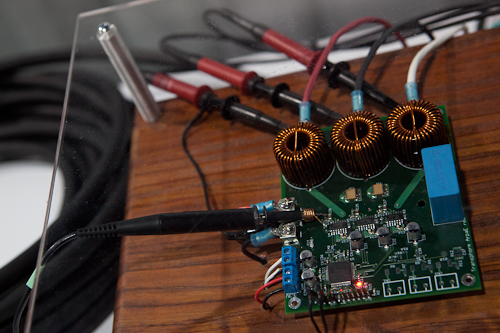
India's Spintronics AI said on October 27 that it is studying a gallium nitride (GaN) chip fab in Ujjain, Madhya Pradesh. The project could cost about ₹2,800 crore (roughly $294 million), with up to ₹800 crore under discussion for the first phase.
The company is evaluating about 40 acres of land, and the state government has issued a letter of intent covering R&D and design support. No final investment decision has been made.
Why it matters: GaN chips are power semiconductors used in chargers, electric vehicles and data center power supplies. India is broadening its chipmaking base with government support.
- GaN (gallium nitride): A semiconductor material that handles higher voltages and faster switching than silicon, used for efficient power conversion.
14. Former TSMC CTO Chenming Hu urges Taiwan to fund universities over state labs

Chenming Hu, the former TSMC chief technology officer best known for inventing the FinFET transistor, argues in his new book that too much of Taiwan's government R&D budget goes to large national research institutes and too little to universities.
He says university research produces both technology and the master's and doctoral graduates industry needs, while the institutes have less multiplier effect and compete with companies for a limited talent pool. He also proposed an outside review of how the R&D budget is spent.
Why it matters: Taiwan's chip strength rests on talent, so a senior industry figure openly questioning how research money is allocated carries weight.
- FinFET: A transistor whose current channel stands up like a fin to reduce leakage; it underpins today's advanced chips.
Sources
- [컨콜]SK하이닉스 "HBM 고객 요청 물량, 공급 가능 물량의 2배 이상" (아시아경제)
- [컨콜] SK하이닉스 "HBM4 수율 계획 상회…목표 상향 조정" (SBS Biz)
- SK hynix (SKHY) Q3 2026 Earnings Call Transcript (The Motley Fool)
- SK하이닉스 “HBM 요청 물량, 공급의 2배…단수 낮춰도 영향 없어” [컨콜] (서울경제)
- Oracle to offer Google TPUs on OCI Cloud from 2027 (IT Brief Australia)
- Oracle Makes the Supercluster Multi-Silicon at AI World 2026 (Futurum Group)
- Google's AI Chips Are Headed to Oracle's Cloud, and The Information Says OpenAI Wants Them Too (WebProNews)
- AMD to Invest $1 Billion in Meta as Companies Expand AI Infrastructure Partnership (The Globe and Mail (보도자료))
- AMD to Invest $1 Billion in Meta Equity as Helios Systems Run at Meta (Securities.io)
- AMD Inks Massive Meta AI Deal To Deploy 6 Gigawatts Of GPUs In Data Centers (HotHardware)
- SK hynix Halts Solidigm IPO Plans (디일렉(The Elec))
- 솔리다임, 美 60조 낸드공장 추진… 곽노정 "주주가치 제고 방향 투자" (파이낸셜뉴스)
- SK Hynix's Solidigm Reportedly In Talks Over $45B Investment In US Chip Plant (Yahoo Finance)
- SK Hynix conditions new US factory on more US chip equipment exports to China, sources say (Reuters (The Standard))
- SK Hynix to time next-generation DRAM shift based on economics (디지털투데이)
- SK Hynix bets on EUV to extend 6F² DRAM as CXMT pushes 4F² (DIGITIMES)
- Chinese Memory Maker's Tech Claim Sinks Samsung, SK hynix Shares (서울경제)
- SK hynix showcases next-generation AI memory technologies beyond HBM (The Korea Times)
- SK hynix Details Memory-Tiering Technologies for AI Inference (TokenPost)
- 聯電第三季營收 742.4 億元創新高,產能利用率衝上 92% 追加 32 億美元資本支出 (TechNews 科技新報)
- 聯電Q3雙率雙升 晶圓出貨創高 (經濟日報)
- 〈精測法說〉Q3獲利翻倍EPS 16.75元創高 全年營收有望年增五成明年續看旺 (鉅亨網)
- 精測財報報喜衝漲停 前三季已賺逾四個股本、午後法說登場 (經濟日報)
- 欣興財報/前三季每股賺17.85元 加碼設備採購509億元 (聯合新聞網)
- 欣興Q3每股賺6.15元 毛利率攀14季高 (工商時報)
- "심텍, 2742억원 규모의 증설로 소캠 생산능력 향상될 것"-키움 (머니투데이)
- 심텍, 충북도ㆍ청주시와 4000억 투자협약…반도체 기판 생산기반 대폭 확대 (이투데이)
- 3M plans ~4.7% stake in GSEO optical collaboration (Stock Titan (3M 보도자료))
- CPO題材點火!3M豪砸48億入股「這檔」拓光通信版圖 (FTNN 新聞網)
- Interview: TI sees liquid cooling shift to tray-level control in AI data centers (DIGITIMES)
- (專訪)液冷走向tray級控制 德儀:散熱系統晶片用量將大增 (DIGITIMES 中文)
- India-based Spintronics AI weighs GaN chip fab in Madhya Pradesh (DIGITIMES)
- Spintronics AI evaluates Rs 2,800 crore GaN semiconductor project in Madhya Pradesh (Manufacturing Today India)
- 張忠謀唯一一次大笑!從錯過英特爾到開創FinFET,胡正明如何「拿出辦法來」助攻台積電登上世界第一 (今周刊)
- 台灣成數位世界基建推手!胡正明:半導體前途大好,育才是當務之急 (遠見雜誌)
Compiled by Bits & Bites from public reporting. Not investment advice.
Leave a Reply