Key takeaways
- Applied Materials to raise Besi stake from 9% to 20%
- Samsung, SK hynix eye 2Q27 for 8-high HBM4 to Nvidia
- DRAM supply seen shrinking up to 50% over 2-3 quarters
- Anthropic S-1 flags reliance on TSMC and HBM makers
- Nvidia secures 2.5x dedicated substrate capacity
- Meta's lease and contract obligations near $825B
- iPhone Duo shipment target reportedly raised 44%
- China's September PPI up 5.0%, fastest since 2022
Watch the video briefing (in Korean)
More briefing videos on our YouTube channel.
1. Applied Materials to raise its Besi stake from 9% to about 20%
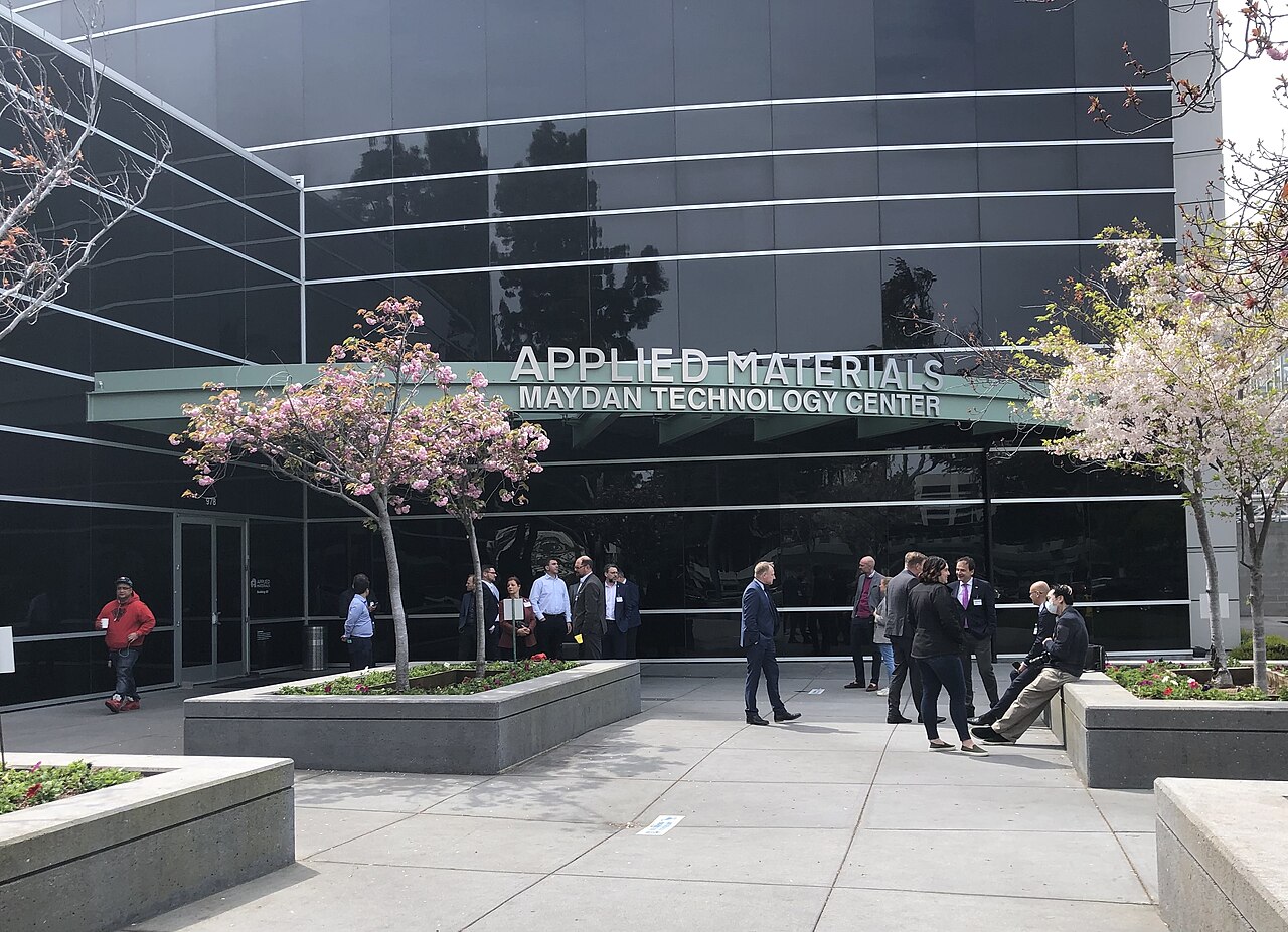
Applied Materials said on October 26 that it will increase its holding in Dutch packaging-equipment maker Besi from roughly 9% to about 20%. The extra shares are being bought through an accelerated share purchase agreement and will be delivered once the US antitrust waiting period ends.
Applied said it does not plan to go beyond about 20% or seek a seat on Besi's board. The two companies have co-developed hybrid bonding equipment since 2020 and launched Kinex, an integrated die-to-wafer hybrid bonding system, in October 2025.
Why it matters: As HBM and chiplet designs stack more dies, hybrid bonding is becoming a core next-generation packaging step. The deal ties the largest equipment maker more closely to a leader in the field.
- Hybrid bonding: A technique that joins the copper contacts of two dies or wafers directly, without solder bumps, allowing denser and thinner stacks.
2. Samsung and SK hynix target 2Q27 for 8-high HBM4 for Nvidia's Rubin Ultra
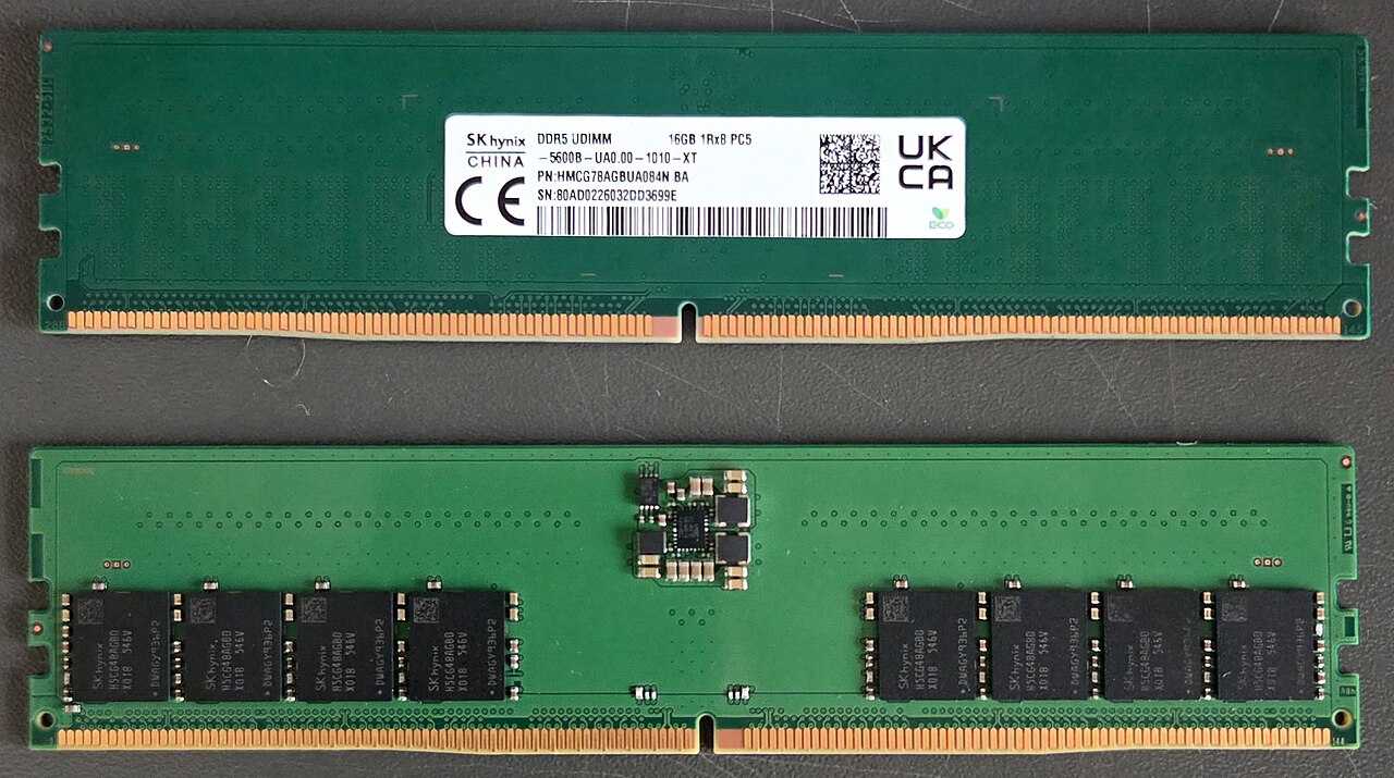
Citing ZDNet Korea, DIGITIMES reported that Samsung Electronics and SK hynix are planning volume shipments of 8-high HBM4 for Nvidia's next-generation Rubin Ultra AI chip starting in the second quarter of 2027.
Taller stacks are running into heat and yield problems, and Nvidia is said to be considering a mix of 8-high and 12-high parts. 12-high HBM4 remains the mainstream product, and the plan has not been confirmed by the companies.
Why it matters: It suggests the HBM race is shifting from simply stacking higher to balancing heat, yield and overall system efficiency.
- HBM: High-bandwidth memory: DRAM dies stacked vertically to move large amounts of data at once, used alongside AI accelerators.
3. DRAM price gains slow as supply is seen shrinking by up to 50%
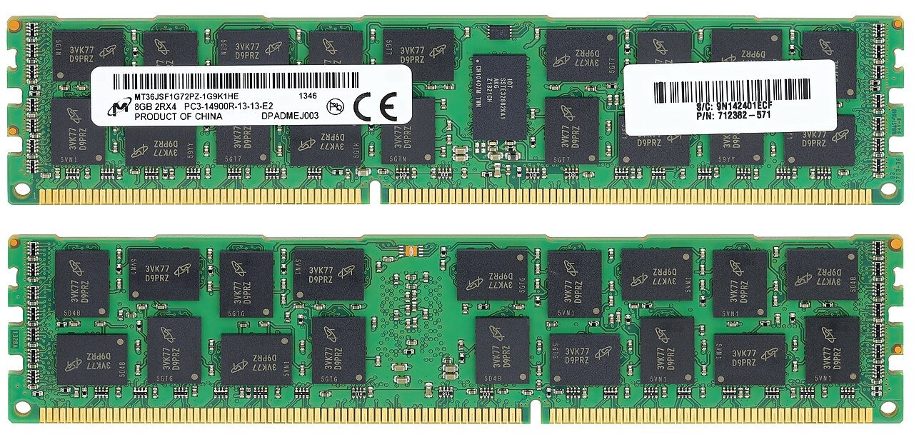
DIGITIMES reported that DRAM price increases slowed sharply in the fourth quarter, yet shortages are worsening as manufacturers restrict shipments. Industry sources expect supply from leading makers to fall 30% to 50% over the next two to three quarters.
That would widen the supply gap heading into 2027. The size of the cut is an estimate from unnamed industry sources.
Why it matters: When allocation matters more than price, customers with long-term agreements gain a clear edge over those without.
4. Anthropic's IPO filing names TSMC and three HBM makers as key risks

Anthropic's S-1, made public on October 26, says that any restriction or delay in advanced chip supply from Taiwan or TSMC would hurt its business. It also flags that HBM supply is concentrated in Samsung, SK hynix and Micron, with production outside the United States.
The filing describes a five-year commitment of $125.2 billion for Broadcom TPU-based compute capacity. Broadcom has agreed to lend up to $42 billion, roughly a third of that amount, and Anthropic noted potential conflicts of interest because Broadcom is both a supplier and a lender.
Why it matters: The filing puts on record how closely an AI model developer's growth is tied to foundry capacity, memory supply and financing.
- S-1: The registration statement a company files with the US SEC before listing, disclosing its business and risk factors.
- TPU: Google's custom AI accelerator, designed and produced with Broadcom's help.
5. Nvidia lines up 2.5x dedicated substrate capacity with six suppliers
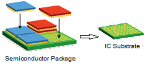
At GTC Berlin on October 21, Nvidia outlined a plan with six suppliers to expand its dedicated package substrate capacity 2.5 times and interposer capacity four times over three years. It did not disclose the baseline, and Ibiden's portion only ramps in 2028.
Taiwan's Economic Daily reported that Intel, Nvidia and AMD have paid deposits totaling more than NT$100 billion to reserve high-end IC substrate capacity. Brokerage forecasts still point to ABF substrate shortages in 2027 and 2028 despite the expansions.
Why it matters: AI chips cannot become finished products without substrates and interposers, so chipmakers are now locking up packaging material capacity as well as wafers.
- ABF substrate: A high-performance package substrate built with Ajinomoto Build-up Film, connecting large chips such as CPUs and GPUs to the board.
- Interposer: An intermediate layer that places chips such as a GPU and HBM side by side and links them with dense wiring.
6. Amkor funds advanced packaging growth with prepayments from 12 customers

Reporting third-quarter results on October 26, Amkor said it has signed advance payment arrangements with a dozen customers since 2025, mainly to support advanced packaging capacity in Korea and Arizona. More agreements are under discussion.
The company narrowed 2026 capex to about $2.5 billion, reflecting the timing of Arizona construction payments, and expects spending to step up in 2027 for facilities in Arizona, Korea and Vietnam. Amkor previously signed a $1.5 billion multi-year agreement with Nvidia, whose prepayment funds US expansion.
Why it matters: Customers paying upfront to reserve capacity is a sign that advanced packaging has become a bottleneck in AI chip supply.
- OSAT: Outsourced semiconductor assembly and test: contractors that package and test chips for others, Amkor being a leading example.
7. Meta's future lease and contract obligations reach about $825 billion
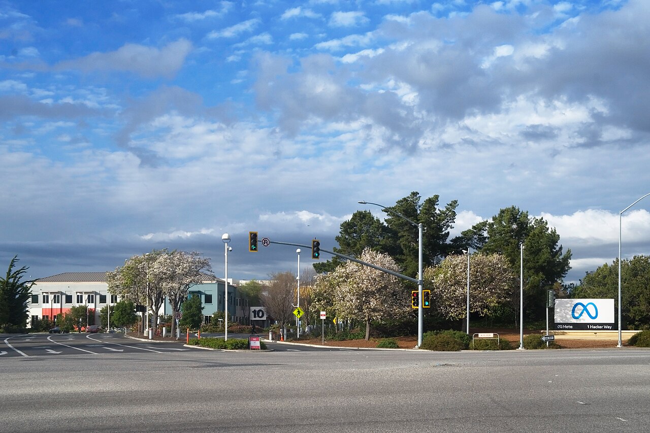
Meta's 10-Q filed on October 22 shows, as of September 30, $454.5 billion in non-cancelable contracts, $355.7 billion in leases that have not yet started, and a cloud purchase commitment of up to $14.7 billion. Bloomberg totaled these at about $825 billion, up from nearly $700 billion in July.
Most relate to AI data centers and compute, with lease start dates running to 2036 and terms of up to 30 years. Meta reported third-quarter capex of $34.9 billion and narrowed its 2026 capex outlook to $135 billion to $145 billion.
Why it matters: The $825 billion is a multi-year total, not annual spending, but it shows how much long-term financial capacity the AI race now demands.
8. Jensen Huang argues GPUs last 8+ years as Nvidia seeks $500B in outside capital

At GTC Berlin, Nvidia CEO Jensen Huang argued that Blackwell and Vera Rubin GPUs could remain useful for seven to eight years or longer, well beyond the roughly four years often assumed in financial models. He pointed to the A100, launched in 2020, as still mission-capable through 2029.
Nvidia said it will work with Apollo, Blackstone, BlackRock, Brookfield, Goldman Sachs and KKR on financing platforms aimed at mobilizing more than $500 billion in third-party capital for AI infrastructure. Longer chip lives mean more collateral value, though some investors are skeptical.
Why it matters: How long GPUs are depreciated over is a central assumption behind data center returns and lending terms.
9. AI server MLCC lead times hit 35 weeks as Samsung Electro-Mechanics eyes Q4 price rises
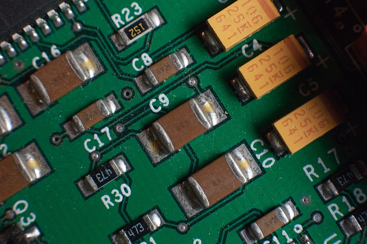
TrendForce data show MLCC lead times in the AI server supply chain rising from 30 weeks in mid-September to 35 weeks in October, nearly three times the roughly 12 weeks seen in a balanced market. Standard lead times for some Samsung Electro-Mechanics parts listed at distributor DigiKey have reached 61 weeks.
In August, TrendForce projected that the company could raise fourth-quarter prices by 25% to 30% for general MLCCs sold to major device makers and by 10% to 20% for AI server parts. Samsung Electro-Mechanics has reportedly pulled forward its new Philippines plant to the first half of 2027.
Why it matters: Longer lead times shift pricing power to suppliers, and even tiny passive components are now a bottleneck for AI servers.
- MLCC: Multilayer ceramic capacitor: a tiny component that stores and releases charge to stabilize voltage; an AI server board uses thousands.
10. AI data center power chips keep 8-inch foundries running flat out
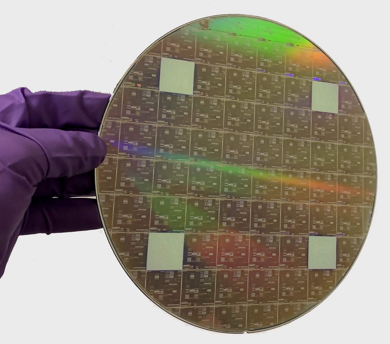
TrendForce expects average 8-inch utilization at the top 10 foundries to approach 90% this year, up from about 80% in 2025, on orders for power management chips and power devices for AI servers, general servers and edge AI. With Samsung and TSMC scaling back 8-inch output, global 8-inch capacity is expected to keep shrinking through the first half of 2027.
South Korea's Herald Business reported that Chinese foundries such as SMIC and Hua Hong have run at full capacity since the start of the year. Industry estimates put SMIC's cumulative 8-inch price increases this year at 10% to 20%, while Hua Hong raised prices 5% to 10% in the first quarter.
Why it matters: Mature-node capacity for power chips, not just leading-edge nodes, is emerging as a new constraint on AI infrastructure.
- Power semiconductor: A chip that converts and regulates voltage and current, used in server power supplies, electric vehicles and more.
11. Fujifilm expands EUV resist output in Pyeongtaek and CMP slurry in Cheonan

According to The Elec, Fujifilm has broadened EUV photoresist production in Shizuoka, Japan, and Pyeongtaek, South Korea, choosing Pyeongtaek, close to its major customers, as its site for leading-edge products. Some products have already passed customer qualification.
Fujifilm has also announced plans to raise CMP slurry capacity at its Cheonan plant by about 30%, with the additional facility due to start in the first half of 2027.
Why it matters: Competition at advanced nodes now extends beyond equipment to local supply of critical materials such as resists and polishing slurries.
- EUV photoresist: A light-sensitive material that records circuit patterns during extreme ultraviolet lithography.
- CMP slurry: A polishing fluid used to flatten wafer surfaces chemically and mechanically.
12. Taiwan's Cheng Mei develops anti-warpage and heat-resistant materials for glass substrates

Polarizer maker Cheng Mei Materials Technology is moving into advanced packaging and developing new materials that help glass substrates resist warping and heat, DIGITIMES reported on October 23. Its dicing and grinding tapes have entered customer verification.
Taiwan News reported that the company is investing more than NT$2.2 billion in semiconductor packaging films and targets mass production in 2028.
Why it matters: Glass substrates depend on more than through-glass vias; process materials that control warpage and heat also determine yields.
- Glass substrate: A next-generation package substrate with a glass core instead of resin, offering less warpage and finer wiring.
- TGV: Through-glass via: tiny holes drilled through glass and filled with metal to connect the top and bottom electrically.
13. Himax and FOCI aim to scale co-packaged optics for AI data centers in 2027
Himax is developing co-packaged optics with Taiwanese optical component maker FOCI using its wafer-level optics (WLO) nanoimprint technology. The first generation targets 1.6T and 3.2T bandwidth, and the second targets 6.4T and is nearing the end of customer validation.
On its second-quarter call, Himax said engineering production began in the third quarter and that the business should contribute more meaningfully from 2027. It added that mass-production timing depends on customers' deployment schedules.
Why it matters: Moving data with light instead of electrical signals is drawing attention as a way past power and bandwidth limits in AI data centers.
- CPO: Co-packaged optics: placing optical transceivers in the same package as a switch or GPU chip to cut power use and signal loss.
14. SK Telecom launches 'Hy-TF' task force for AI work with SK hynix
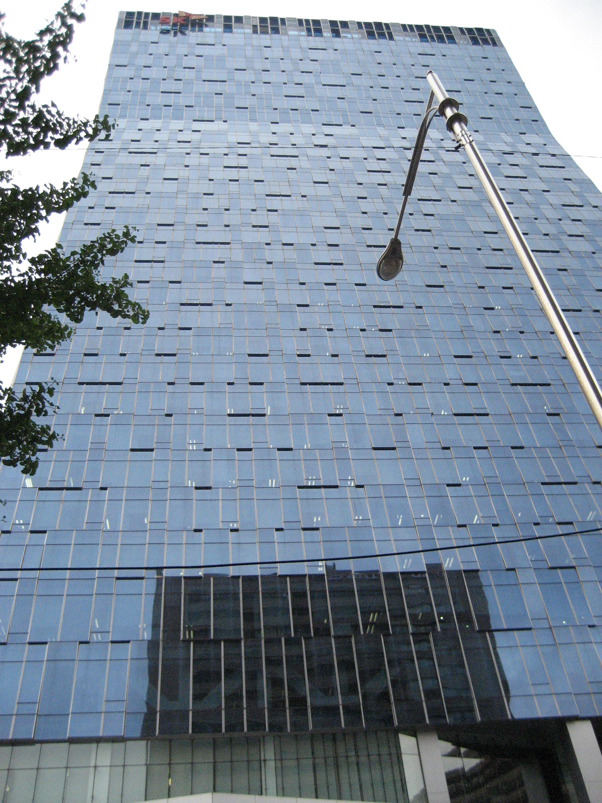
According to the Electronic Times, SK Telecom has set up Hy-TF, a task force under its AI company-in-company dedicated to AI collaboration with SK hynix. The group has about 20 executives and leaders and is headed by AI CIC chief Yoo Kyung-sang.
Hy-TF will advance AI-driven manufacturing automation, including digital twins of chip fabs built on Nvidia Omniverse, as part of SK hynix's goal of an autonomous fab by 2030. SK Telecom also plans to turn its manufacturing AI data platform into a business serving outside companies.
Why it matters: It is an attempt to package fab operating know-how into AI solutions that can be sold to other manufacturers.
- Digital twin: A virtual replica of a real factory or piece of equipment used for simulation and optimization.
15. HCLTech and Rapidus open two 2nm engineering centers in India
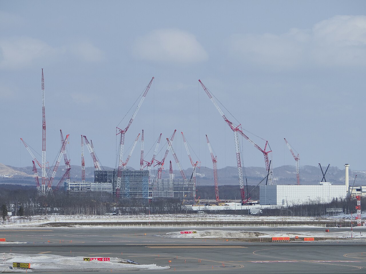
Indian IT firm HCLTech and Japanese foundry Rapidus opened two development centers in Bengaluru and Hubli on October 26. The centers cover mask design, design infrastructure, PDK development, DTCO and layout design.
HCLTech will also help build a pipeline of Indian engineers for Rapidus's needs in Japan. Rapidus plans to release PDKs in fiscal 2026 and begin 2nm mass production at its Chitose plant in Hokkaido in fiscal 2027.
Why it matters: A new foundry needs an ecosystem of design tools and support engineers to win customers, and Rapidus is turning to India's design talent to build it.
- PDK: Process design kit: the design rules and device models a foundry gives customers so they can design chips for its process.
- DTCO: Design-technology co-optimization: tuning circuit design and manufacturing process together to improve performance and area.
16. TI sees $500 to $1,000 of its chips in each humanoid robot
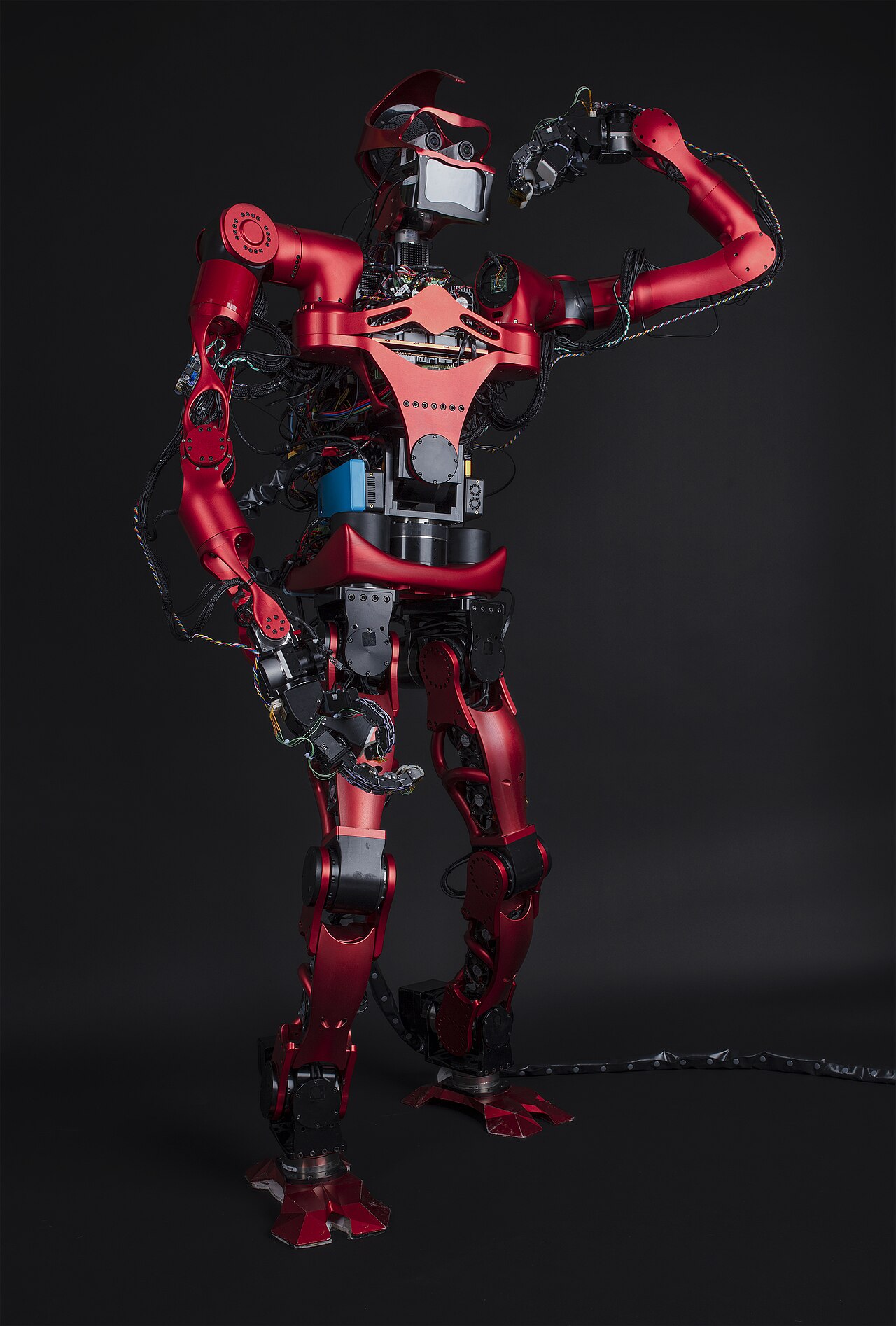
Texas Instruments estimates that each humanoid robot could carry $500 to $1,000 worth of its semiconductors, and it expects robot production to pick up from 2027.
TI is promoting gallium nitride power devices, C2000 real-time microcontrollers and precision analog parts for joint and hand designs.
Why it matters: Robots that must control many motors precisely use large numbers of sensing, power and control chips, making physical AI a new demand source for analog semiconductors.
- GaN: Gallium nitride: a semiconductor material that converts power faster and more efficiently than silicon.
17. Apple reportedly lifts 12-month iPhone Duo shipment target by 44%

DIGITIMES reported that strong preorders led Apple to raise its 12-month shipment target for the iPhone Duo, its first foldable, from 9.7 million to 14 million units, an increase of about 44%. Apple has not confirmed the figures.
Earlier reports described production problems in assembly, displays and hinges before launch, and display issues have surfaced again, so actual shipments will depend on yields.
Why it matters: The target only turns into shipments if foldable panel and hinge yields hold up, with knock-on effects across the display and component supply chain.
18. SpaceX in talks for 80,000 US cell sites to expand Starlink Mobile

Bloomberg reported that SpaceX is negotiating access to at least 80,000 cell sites in the United States, about half of the country's purpose-built towers. No deal has been signed.
On October 8, SpaceX agreed to buy Grain Management's 800MHz spectrum, a deal expected to close in the first half of 2027 pending regulatory approval. The FCC has also approved 15,000 next-generation direct-to-cell satellites.
Why it matters: A hybrid network combining satellites and ground towers could reshape demand for telecom chips and handsets.
- Direct-to-device: Satellite service that connects ordinary smartphones straight to satellites without special hardware.
19. China's September producer prices up 5.0%; Kingboard raises laminate prices 15%

China's National Bureau of Statistics said September producer prices rose 5.0% year on year, the fastest pace since June 2022, driven mainly by crude oil and non-ferrous metals. Consumer prices rose only 0.9%.
Hong Kong laminate maker Kingboard raised prices on copper-clad laminate and prepreg made with 2116 or thinner glass cloth by 15% on October 13, its eighth increase this year.
Why it matters: Rising material costs alongside flat consumer prices widen the gap between AI-related industries that can pass on costs and consumer sectors that cannot.
- Copper-clad laminate (CCL): An insulating board of glass fiber and resin covered with thin copper foil, the base material for printed circuit boards.
- Prepreg: Resin-impregnated glass fiber sheets used to bond circuit board layers together.
20. Vietnam's first chip fab may miss its 2027 trial production goal
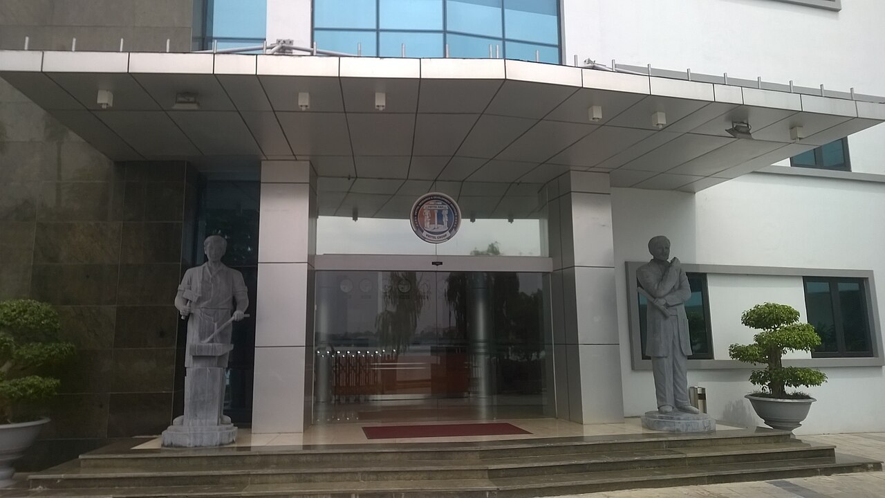
Reuters, citing people familiar with the project, reported that state-owned Viettel's fab, Vietnam's first, is unlikely to start trial production in 2027 as planned. Talks with ASML over deep ultraviolet lithography equipment have dragged on for months, and satellite images show the site still undeveloped.
Sources blamed limited fab-building experience and slow government funding approvals. Viettel said the project is on track, and ASML declined to comment. Authorities put the plant's cost at about $1.3 billion, with full operation targeted for 2030.
Why it matters: Money alone cannot build a fab; securing key tools and process know-how sets the timeline.
- DUV: Deep ultraviolet lithography: patterning tools using longer wavelengths than EUV, widely used at mature nodes.
21. Tamil Nadu offers chip subsidies even to projects without central approval
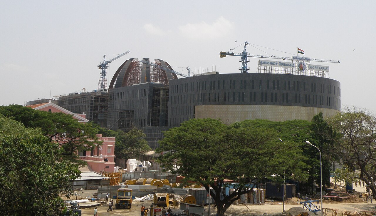
India's Tamil Nadu state launched its Semiconductor Ecosystem Scheme 2026 in October. Projects approved under the central government's Semicon 2.0 program receive an additional 15% to 25% of approved capital spending from the state.
Projects that did not apply or were not selected can use a separate track offering fixed capital subsidies of 15% to 25% of eligible assets plus up to 2% of turnover a year for five years. Wafer fabs, advanced and legacy packaging, materials, equipment and testing facilities qualify, with minimum investments of Rs 50 crore to Rs 500 crore and applications due by September 30, 2027.
Why it matters: Indian states are now competing for chip investment with their own incentives, separate from national support.
Sources
- Applied Materials to raise BESI stake to about 20% (Reuters (Euronext))
- Applied Materials Agrees to Raise Besi Stake to ~20% (StockTitan (회사 보도자료))
- Samsung, SK Hynix eye 2Q27 shipments of 8-layer HBM4 to Nvidia (DIGITIMES)
- Samsung & SK hynix Reportedly Set To Ramp 8-Layer HBM4 Shipments For NVIDIA's Rubin Ultra In Q2 2027 (Wccftech)
- DRAM price gains fall short as supply shrinks up to 50% (DIGITIMES)
- Anthropic Flags HBM Supply Risk From Samsung, SK hynix in IPO Filing (Seoul Economic Daily)
- Anthropic's IPO filing puts TSMC and HBM suppliers at the center of its risk story (Crypto Briefing)
- Broadcom faces scrutiny over $42 billion Anthropic loan in IPO filing (Crypto Briefing)
- Anthropic's IPO plans: 900% revenue retention, but $80 billion in first-half losses (CNBC)
- Nvidia locks in 2.5x substrate and 4x interposer capacity with six suppliers (Silicon Analysts)
- High-end IC substrate capacity pre-orders (Economic Daily report) (36Kr)
- ABF 產能缺口 (ABF production capacity) (TechNews)
- Amkor (AMKR) Q3 2026 Earnings Call Transcript (The Motley Fool)
- Nvidia backs Amkor with $1.5bn to expand AI packaging in the US (eeNews Europe)
- Meta reports $825B in future lease and contract commitments (The Next Web)
- Meta Platforms, Inc. – Form 10-Q (Q3 2026) (SEC)
- Jensen Huang says Nvidia AI chips carry lowest risk (TechSpot)
- Jensen Huang says Blackwell and Vera Rubin GPUs could stay useful for seven or eight years (Crypto Briefing)
- Nvidia is setting up a $500B program for AI infrastructure with likes of BlackRock, Goldman Sachs (Blockspace)
- 삼성전기 MLCC '납기 61주'…가격 주도권도 쥔다 (뉴스핌)
- AI power chip orders surge as global 8-inch capacity shrinks (헤럴드경제)
- Capacity Cuts and Surging Demand for AI Power ICs Set Stage for Mature-Node Foundry Price Increases, Says TrendForce (TrendForce)
- 후지필름, 평택 거점 EUV PR 양산 채비…삼성전자 초밀착 공조 (디일렉)
- 日 후지필름, 2027년까지 평택·천안 등에 반도체 소재 설비 투자 (전자신문)
- 誠美材布局先進封裝 開發新品助玻璃基板抗翹、耐熱 (DIGITIMES)
- Cheng Mei Materials invests over NT$2.2 billion in semiconductor packaging films (Taiwan News)
- Himax Technologies Q2 Earnings Call Highlights (MarketBeat)
- [단독] SK텔레콤, 하이닉스 AI협력 전담 'Hy-TF' 가동…TF장에 유경상 CIC장 (전자신문)
- Inside SKT's push to turn SK Hynix's fabs into an AI business (DIGITIMES)
- Rapidus partners with Indian tech giant on chip development (The Japan Times)
- HCLTech and Rapidus open India centers to support semiconductor engineering (DIGITIMES)
- Texas Instruments sees $500 to $1,000 chip content per humanoid robot (Crypto Briefing)
- Exclusive: Apple raises iPhone Duo shipment target 44% on strong preorders (DIGITIMES)
- Weekly news roundup: iPhone Duo shipment target revised upward amid display issues (DIGITIMES)
- Apple Reportedly Boosts iPhone Duo Orders by 44% (MacRumors)
- SpaceX Wants 80,000 Cell Sites to Make Starlink Mobile a Real Carrier (Tesla North)
- SpaceX Seeks 800 MHz Spectrum to Make Starlink Mobile a Major US Carrier (eWeek)
- SpaceX Expands Starlink Mobile With 800 MHz Spectrum Deal And FCC Approval For 15,000 Satellites (Pulse 2.0)
- Consumer Price Index in September 2026 (중국 국가통계국)
- China PPI rise fastest since June 2022 on fuel costs (CNBC)
- PCB laminate price increase and quote impact (NextPCB)
- Sources: Vietnam's first chip plant has not reached an agreement with ASML, making the 2027 target unlikely (Shanghai Metals Market (Reuters 인용))
- Vietnam's First Chip Plant Timeline Looks Like It's Slipping (Finimize)
- TN announces semiconductor scheme; offers up to 25% subsidy (DT Next)
Compiled by Bits & Bites from public reporting. Not investment advice.
Leave a Reply